Graphics Card Schematic Diagram
Anyways, the schematics aren't public since card makers have to invest time and money to come up with those designs. Well the fps of the windows 3d games is suffering a lot due to the low isa bus bandwidth.
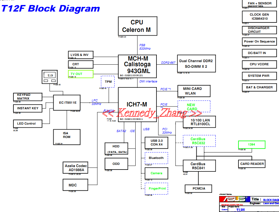
Asus X51H (T12F,T12H) schematic Laptop Schematic
Traces and vias) and the pg413 reference schematic.

Graphics card schematic diagram. 4 attachment (s) here i have the gtx 1080 reference nvidia schematic that i got from some random website. Circuits to transmit and demoludate rf / video signals over fibre optic cable: Gpus as storage system accelerators | massively multicore processors, such as graphics processing units (gpus), provide.
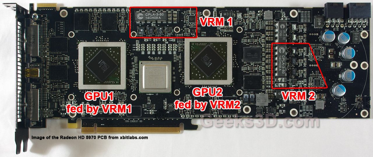
In addition, i will also provide the msi gtx 1060 pg410 schematic. Here is the diagram of a hd 5970 vrm: Schematic diagrams schematic diagram is a fundamental two dimensional circuit representation showing the functionality and connectivity between different electrical components.
This component allows to adjust the gpu voltage up to 2.0v (and adjusting the voltage of each gpu separatly is possible in theory…). Graphics card schematics and boardviews. The default voltage is 1v.
I will check and upload it if that is the case. There no point on a gpu schematics and for sure they will never be released. The latest pci express specification places limits as to how much current can be drawn, in total, off the two sets of voltage lines.
The hd 5970 voltage controller is a volterra vt1165mf. The gpu (the chip) is made by amd. For modern graphics cards, it's 3 amps off the +3.3v lines and.
Igor's lab leaked a system architecture diagram and board design diagram of the intel dg2 discrete graphics card today, and there are plenty of highlights. Occasionally some schematics do appear on the internet, but they are few and far between. You basicly need no schematics as what can be bad are the ic itn self, the ram ic or the vrm which can be check with no schematics.
But then again, the windows 98 era goes hand in hand with pci graphics cards. Provides circuit diagram, schematic diagram、boardview,maintenance case, include mobile phone, tablet, laptop, graphics card, motherboard and server. The riva 128 introduces the most , serial interface · bus mastering dma 66mhz accelerated graphics port.
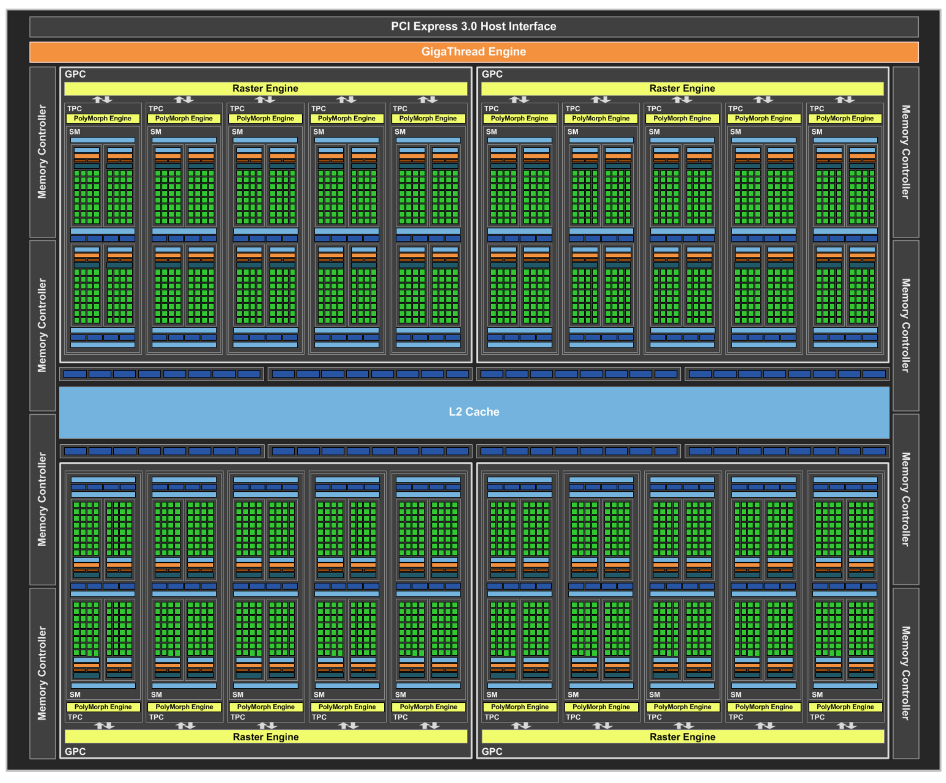
The basic vga display modes of 80x25 character mode and 640x480 in graphics mode are still supported by all modern graphic cards, independent of the extended modes supported by these cards. Download scientific diagram | gpu schematic architecture. For sure reflow the gpu no solve the issue, remove and change it make no sense.
About the metal inner frame 0.8+1.0+1.5mm blackened steel structure the internal structure is finished with a matt black coating. Further, that part number you supplied is for the gpu (the chip itself), not for the whole video card. Requirements of the mainstream pc graphics market and microsoft's pc'97.
Vga (video graphics array) video graphics array is a computer display standard using analog signals proposed by ibm in 1987. Vga interface pin definition_ schematic diagram of vga interface wiring method. The schematic diagram and the zipped gerber files for this card can be downloaded from the links provided above.
I'm currently waiting on the boards for card c to arrive from the pcb manufacturer. Samsung dvd schematic circuit diagram mk2715 ccir656 ks0127 schematic nvidia graphics card yuv12 samsung flyback pin diagram riva 128 1995 philips vmi connector. The widespread adoption has since made this the baseline for all displays and is still the baseline for operation today.
Tv rgb signal output from a svga graphics card: Due to its smooth finishing characteristics, only the original spray powder can be used to avoid the. What is pcie 4.0 x12?
What i require from you is one push of your right index finger on the upvote button i'll give you a link to a. Card a is still in the pcb layout phase. Intel dg2 discrete gpu schematic leaked:
If you have a question about the best card in the market or just what card is right for you, will answer it. Very helpful and will definitely come in handy. Vga interface is a special interface for computers to output data using vga standard.
206 x 124 x 46 mm. Video graphics array (vga) is a video standard devised by ibm for their ps/2 computers in 1987. This subreddit is for build questions and graphics cards.
I've got a secret, and it's gonna cost you. Tip:username no bind computer, no restrict ip login, any pc and ip can login. The standard specifies a set of screen resolutions, operating modes, and minimum hardware requirements.
It includes the gencad format pg413 pcb boardview (incl. Schematics for gpus are probably impossible to find. Pic pal video library including source code and circuit schematics:
It is vital for a pcb designer to get familiarized with the schematic symbols that represent the components on a schematic diagram. Vga interface has 15 pins and is divided into 3 rows with 5 holes in each row. Join free, you can try it.

The structure of VGA Graphic Card. Download Scientific

Schematic visualization of a GPU device. Download
[Tutorial] Graphics Card Voltage Regulator Module (VRM
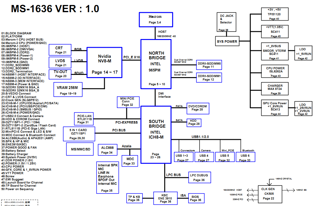
MSI EX600 schematic, MS1636 Laptop Schematic
Graphics card pcb diagram for components AskElectronics

EVGA GTX 1080 Ti SC2 ICX Review vs. Gaming X, Xtreme Aorus
Need ic name/schematic diagram Graphics Cards Linus
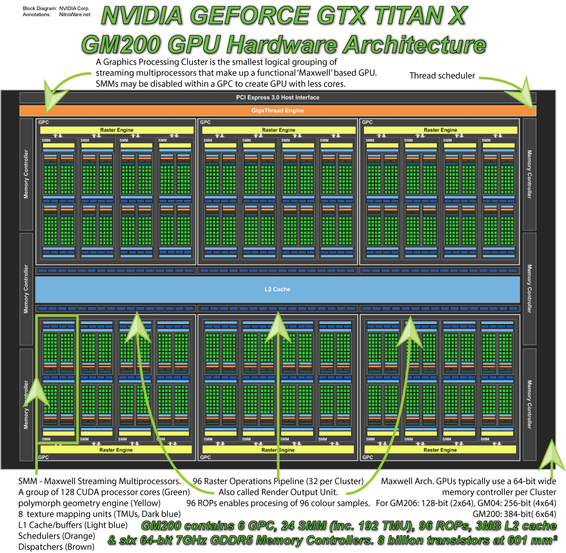
NVIDIA GeForce GTX TITAN X Video Card
![]()
Pci Express Wiring Diagram pcie sense pin pcie 8 pin
285 GPU VID after volt mod. EVGA Forums

GeForce GTS 240 schematic diagram exposed

MSI R9 390X vrm and mem chip cooling Graphics Cards
Hardware
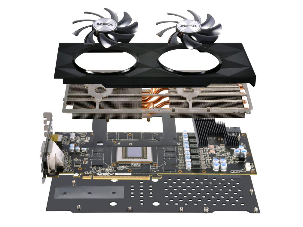
XFX Radeon R9 390 Black Edition OC 8GB Video Card Review
Masochist's Video Card Schematic PyroElectro News
Schematic Design Methods Multiline Designs


How To Read Printed Circuit Board Diagram Tech India Today

Late 2013 Mac Pro System Block Diagram Desktop Computing
Nvidia GeForce GTX 1080 review The most badass graphics