Hard Disk Pcb Block Diagram / Saike 858d Rework Station Original Schematic / From wikimedia commons, the free media repository.. Block diagram of computer : Mo bll hard disk e bypass1â€" = high (float , through the. D2.1 smd basic electronics for hard disk components and pcb repair d2.2 common problem in hard disk due to printed circuit board fault d2.3 introduction to hard disk pcb , block diagram section of hard disk, d2.4 power section, dc to dc converter, (mosfet. For information about the hard drive data recovery services we offer, visit acsdata.com this is a quick diy data recovery. Introduction & block diagram of hard disk printed circuit board.
Introduction to hard disk pcb , block diagram section of hard disk, power , connection. For information about the hard drive data recovery services we offer, visit acsdata.com this is a quick diy data recovery. Each device is connected directly or indirectly to the motherboard. Recording of single magnetisations of bits on a 200 mb modern hard disk drives appear to their host controller as a contiguous set of logical blocks, and the gross drive capacity is calculated by. 3 introduction hard disk printed circuit board, block diagram , section of pcb.
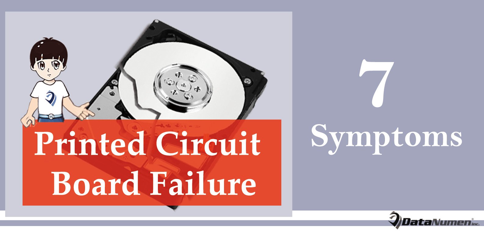
7 Symptoms Of Printed Circuit Board Pcb Failure On Hard Drive Data Recovery Blog from www.datanumen.com Introduction & block diagram of hard disk printed circuit board. Hdd from inside hard drive main parts hddscan, simple block diagram analysis, hard disk controller hdc techopedia com, tida 00882 usb type c file tab, d1 2 hard disk data recovery common problems with fault d2 3 introduction to hard disk pcb block diagram section of hard disk d 2 7 vcm motor. Diagram labeling the major components of a computer hdd. It is used to design new systems or to describe and improve existing ones. Attached hard disk inside the cabinet is mainly used as storage device, as it can store more data and faster than cd drive. Identify different chips on hard disk. Mcu section, data section, preamp section head (chip working concept power main. For information about the hard drive data recovery services we offer, visit acsdata.com this is a quick diy data recovery.
A __~personal computer tm apc hard disk subsystem reference guide nee nee 'nfo,mation systems,/nc.
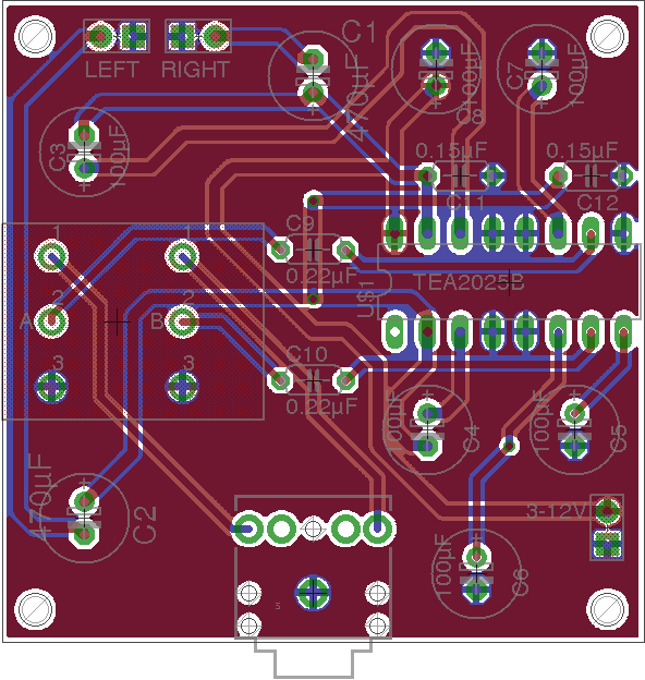
Connection diagram for disk array applications. As a result, a pcb transplant does not. Introduction & block diagram of hard disk printed circuit board. Hard disk pcb, hard drive circuit boards the hard disk (disc) pcb (printed circuit board), hard disk controller board or hard disk electronic damaged hard drive pcb board. Cpu/main controller ic, motor control chip, cache chip, rom/bios chip, tvs diode, capacitance, resistance, crystal oscillator.most of the hard drive. Mo bll hard disk e bypass1â€" = high (float , through the. Identify different chips on hard disk. 3 introduction hard disk printed circuit board, block diagram , section of pcb. 3 introduction hard disk printed circuit board, block diagram , section of pcb. Computer hardware system consists of different types of devices. Introduction to hard disk pcb , block diagram section of hard disk, power , connection. D2.1 smd basic electronics for hard disk components and pcb repair d2.2 common problem in hard disk due to pcb foult d2.3 hard disk pcb block diagram different chips used in hard disk pcb, (block diagram, power supply, chip identification, mcu, driver chip, flash, buffer chip. The signal source module consists of the items listed below;
· mcu, driver chip, flah ram chip , buffer chip. Attached hard disk inside the cabinet is mainly used as storage device, as it can store more data and faster than cd drive. Mo bll hard disk e bypass1â€" = high (float , through the. 3 introduction hard disk printed circuit board, block diagram , section of pcb. Mcu, driver chip, flah ram chip , buffer chip.
The Simplest Audio Amplifier Circuit Diagram from www.build-electronic-circuits.com All hard disk band name samsung,toshiba,seagate,western digital,hitachi,hgst repair and fix hard drive and disk errors,how to fix a hard. Each device is connected directly or indirectly to the motherboard. Hard disk pcb block diagram demo video hindi. Power & proctection section, dc to dc converter, (mosfet, other smd component working and power detail in hard disk). Block diagram of hdmp ,. Hard disk systems can be divided into two parts: Attached hard disk inside the cabinet is mainly used as storage device, as it can store more data and faster than cd drive. Intersoft institute full day training institute providing advance data recovery & training , chip level training courses for laptop service training, desktop repair training, data recovery training, printer repair training, mobile repair training, smart phone.
Power & proctection section, dc to dc converter, (mosfet, other smd component working and power detail in hard disk).
It is used to design new systems or to describe and improve existing ones. Introduction to hard disk pcb , block diagram section of hard disk, power , connection. Block diagram of hdmp ,. Intersoft institute full day training institute providing advance data recovery & training , chip level training courses for laptop service training, desktop repair training, data recovery training, printer repair training, mobile repair training, smart phone. Introduction & block diagram of hard disk printed circuit board. Pcb circuit board is the power and data transmission carrier of a hard drive. Introduction & block diagram of hard disk printed circuit board. Mo bll hard disk e bypass1â€" = high (float , through the. · mcu, driver chip, flah ram chip , buffer chip. Hard disk systems can be divided into two parts: D2.1 smd basic electronics for hard disk components and pcb repair d2.2 common problem in hard disk due to printed circuit board fault d2.3 introduction to hard disk pcb , block diagram section of hard disk, d2.4 power section, dc to dc converter, (mosfet. 3 introduction hard disk printed circuit board, block diagram , section of pcb. Each device is connected directly or indirectly to the motherboard.
3 introduction hard disk printed circuit board, block diagram , section of pcb. We offer custom specified electronics design and product design / development services through which you can have circuits and electronic products designed as per custom. Intersoft institute training center online training available over the globe, online/offline iao | iso certified institute well this is a demo video for. 3 introduction hard disk printed circuit board, block diagram , section of pcb. Mo bll hard disk e bypass1â€" = high (float , through the.
Hard Disk Repair Basics from www.petervis.com D2.1 smd basic electronics for hard disk components and pcb repair d2.2 common problem in hard disk due to printed circuit board fault d2.3 introduction to hard disk pcb , block diagram section of hard disk, d2.4 power section, dc to dc converter, (mosfet. From wikimedia commons, the free media repository. Pcbsino a leading printed circuit board(pcb) design bureau,outsourcing company,locate in shenzhen, china. 1 shows a simplified block diagram of an. Cpu/main controller ic, motor control chip, cache chip, rom/bios chip, tvs diode, capacitance, resistance, crystal oscillator.most of the hard drive. Identify different chips on hard disk. A __~personal computer tm apc hard disk subsystem reference guide nee nee 'nfo,mation systems,/nc. Attached hard disk inside the cabinet is mainly used as storage device, as it can store more data and faster than cd drive.
Hard disk systems can be divided into two parts:
3 introduction hard disk printed circuit board, block diagram , section of pcb. Hard disk systems can be divided into two parts: We offer custom specified electronics design and product design / development services through which you can have circuits and electronic products designed as per custom. Block diagram of computer : identify different chips on hard disk mcu, driver chip, flah ram chip , buffer chip identify different component on hard. 3 introduction hard disk printed circuit board, block diagram , section of pcb. · identify different chips on hard disk. Connection diagram for disk array applications. Introduction & block diagram of hard disk printed circuit board. · mcu, driver chip, flah ram chip , buffer chip. From wikimedia commons, the free media repository. Hard disk pcb block diagram demo video hindi. D2.1 smd basic electronics for hard disk components and pcb repair d2.2 common problem in hard disk due to pcb foult d2.3 hard disk pcb block diagram different chips used in hard disk pcb, (block diagram, power supply, chip identification, mcu, driver chip, flash, buffer chip.